Our attitude towards innovative thinking, an uncompromising customer-oriented mindset, immediate market proximity, and
its availability make us who we are and present an opportunity to serve the customers in front of us.
We identify innovative methods based on the finding of the problems which remain and remained unidentified in front of
many eyes for a long time. With our innovative solutions, smart products, and individual services, we strive to solve
problems that have been identified and exceed the customers' requirements.
Successful inventions are being integrated into the products at OSEPL, Daund, using our reliable but very common senses
for future technological and market requirements. When both converge, the product reaches a higher level of quality.
OUR CONTRIBUTION TO THE IMAGING WORLD
HRHS-AI®: It stands for "High Resolution High Speed through Alternate Imaging (HRHS-AI)".Our invented method has been standardized under SLVS-EC by the Japan Industrial Imaging Association for sensor manufacturing.
SLVS-EC stands for "scaler low voltage signaling with embedded clock". Sensors have been designed and manufactured by
Sony Semiconductor Solutions Group in such a manner that they are now ready for implementation of our invented method as mentioned
in our patent publication (IN201927044969, PCT/IN2018/050558, WO2019/053739). Sony has manufactured sensors that allows
us to deliver high speed and high resolution images without addition of any pin or any additional support.
Multi lane functionality adds another dimension to the high speed imaging. For full fledge practical implementation,
for us, there is a need of already existing boards or development and manufacturing of new electronic circuit from our side.
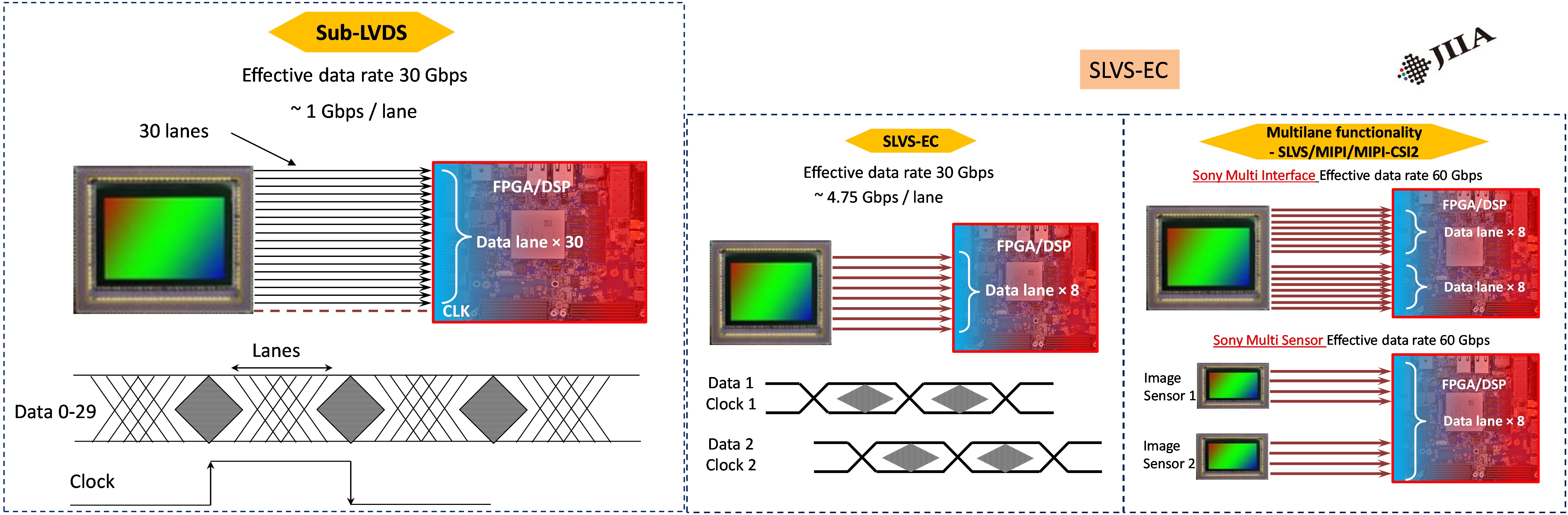
Figure 1 shows a sub-LVDS system employed for high speed data acquisition. With 1 clock lane and 30 data lane and 1 Gbps / lane, the data acquired is of 30 Gbps.
Camera systems including the mobile phones, accommodate the image sensors which fall under the category of sub-LVDS system and employ the alternate imaging pattern / technique covered under the IN201927044969 regardless of alternate arrangement/s made to achieve it either partially or completely.
This is owing to the fact that the data acquisition or image acquisition in an alternative imaging pattern is the key. Thus the cameras based on such sensors are claimed by us. Some sensors are manufactured with LVDS channels.
The cameras and mobile phones based on sensors with LVDS channels are also claimed by us wherever the additional electronic interfaces may shift those sensors to the sub-LVDS or SLVS category.
Several Gpixel sensors are manufactured in such a way that data can be acquired in an alternate imaging pattern as invented by OSEPL, Daund.
The data acquisition can be improved further with our method as displayed in figure 2 under the trade name SLVS-EC. In this case only 8 data lanes can be used to transfer 30 Gbps in contrast to the
data acquisition in sub-LVDS system. Here, one sensor with multiple data lanes enables a fast and easy data transmission at around 30 Gbps with 5 Gbps / lane.
It has a featured embedded clock that makes data acquisition even with the unequal data wire lengths. Even without a clock lane,
SLVS-EC makes us have a greater freedom around our method that has been described in patent publication. This is a MonoCam version of our imaging solution.
Figure 3 shows two versions of the image acquisition system under the multilane functionality with SLVS-EC and MIPI or MIPI CSI mode.
First one is a multi interface version and the second one is a multi-sensor version causing the image data transfer rate as high as 60 Gbps onwards. In the multi-sensor version,
sensors are mounted on a 50-50 beam splitter prism to enable the images at 60 Gbps. This is a TwinCam version of our imaging solution using a prism mounted image sensor arrangement.
This is the same as our multi stream functionality technique with memory segmentation or pixel cluster allocation to different lanes and the data collection form the segmented pixel clusters.
We have imaging solutions in MonoCam and TwinCam mode with multilane functionality. The contemporary image sensors leverage the patented techniques
outlined in patent number 480945 (201721015412) to effectively capture sensor image data for HRHS-AI. Our invented method has been extensively exploited in
a sub-LVDS configuration with multilane connections synchronized over a single clock signal, facilitating purposeful delay generation and obviating
the necessity for numerous clock lanes. Skew adjustments (and not mere the arrangements) have been supplanted by integrated embedded clocks of
SLVS-EC, leading to a more compact sensor package and enabling rapid data transmission. Our inventions led to the manufacturing of the fastest image sensors till this date.
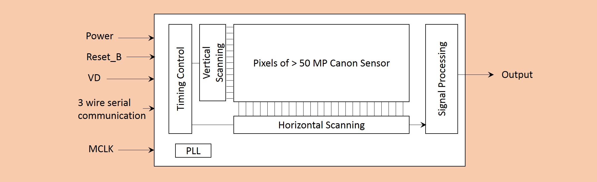
In case of all low FPS imaging sensors which give more than 50 MP resolution, our method is used for high speed scanning of vertical or horizontal pixel arrays.
Several combinations can be made to employ our invented methods. Data acquisition from alternate pixel rows or columns can be done by arranging the alternate clocking or switiching.
Pixel groups can be given the alternate triggers to acquire data. Image sensors with more than 50 MP resolution used for
single shot static imaging in mobile phones employ this method. The architecture is as shown in the following figure.
HRHS-AI® for other electronic devices / ICs
Qualcomm Snapdragon, MediaTek Dimensity, Apple A17 Pro, Tensor G3, Google tensor, Kirin 9000, Exynos 2100, Unisoc T820, Helio G99 etc. Further examples of the integrated circuits and devices are - Intel, Celeron, Pentium, Xeon, DAQ systems/digitizers etc.